
Happening this week is the IEEE’s annual VLSI Symposium, some of the business’s primary occasions for disclosing and discussing new chip production ways. Some of the expected shows scheduled this yr is from Intel, who’s on the display to stipulate the bodily and function traits in their upcoming Intel 4 task, which might be used for merchandise set to be launched in 2023. The improvement of the Intel 4 task represents a important milestone for Intel, because it’s the primary Intel task to include EUV, and it’s the primary task to transport previous their stricken 10nm node – making it Intel’s first likelihood to get again heading in the right direction to re-attaining fab supremacy.
Intel’s scheduled to ship their Intel 4 presentation on Tuesday, in a chat/paper entitled “Intel 4 CMOS Generation That includes Complicated FinFET Transistors optimized for Prime Density and Prime-Efficiency Computing”. However this morning, forward of the display, they re publishing the paper and all of its related figures, giving us our first have a look at what sort of geometries Intel is achieving, in addition to some extra details about the fabrics getting used.
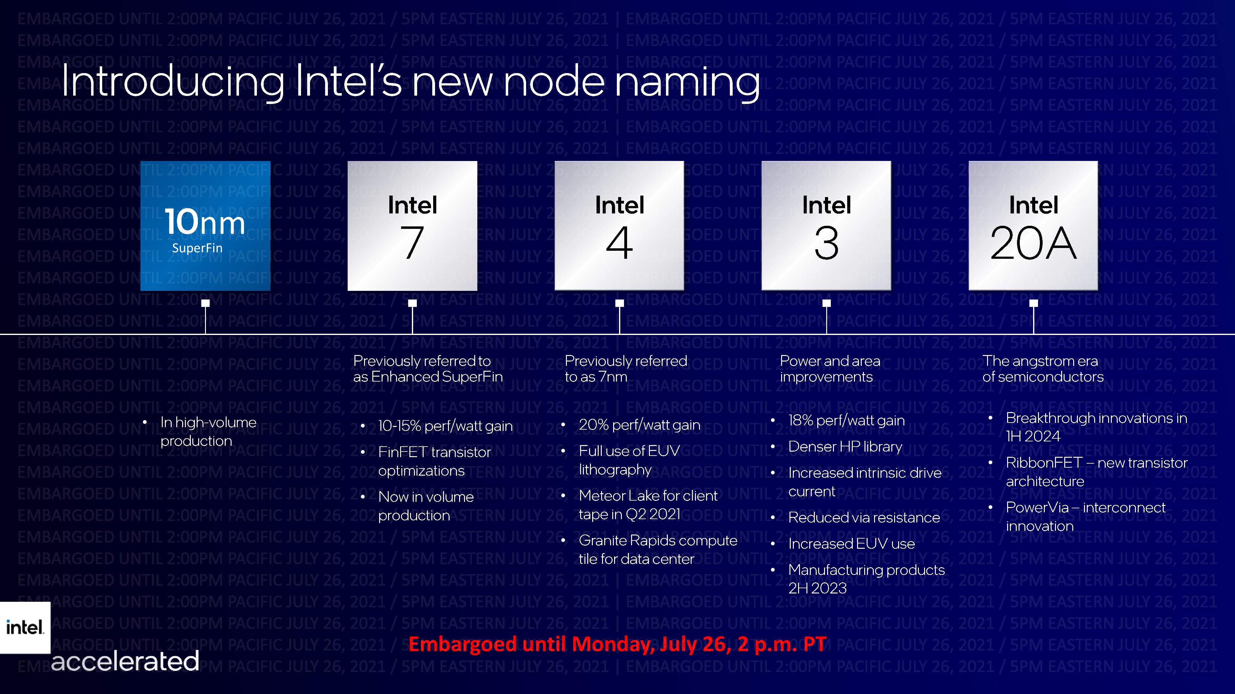
Up to now referred to as Intel’s 7nm task, Intel 4 is Intel’s first time the use of EUV lithography for his or her chips. A very long time coming, the usage of EUV guarantees each to permit Intel to attract the type of ever-smaller options wanted for extra complicated production nodes, whilst on the similar time letting Intel lower down at the selection of production steps required by means of as of late’s multi-patterning DUV ways. Strangely, Intel reveals itself as the overall of the large 3 fabs to faucet into EUV – the corporate handed on EUV for the 10nm era as they didn’t really feel it was once in a position, after which delays with 10nm and 7nm driven again Intel’s EUV adoption level considerably. In consequence, Intel gets to spring ahead at the foundation of EUV-driven beneficial properties, although they’ll nonetheless must make up for misplaced time and TSMC’s revel in benefit.
The improvement of Intel 4 may be a important juncture for the corporate, because it in spite of everything lets them transfer previous their stricken 10nm task. Whilst Intel has controlled to make one thing appropriate in their 10nm task nodes – particularly with their most up-to-date 10nm Enhanced SuperFin variant, which we higher know as Intel 7 – it’s no longer been with out completely an excessive amount of blood, sweat, and years. Intel believes they attempted to do an excessive amount of all of sudden with 10nm – each with reference to scaling and in too many new production ways – which in flip set them again years as they untangled that mess to seek out and iterate on what went incorrect. Unsurprisingly then, Intel is being a little bit much less competitive with their first EUV node, and the corporate general has taken a a lot more modular construction method going ahead, taking into consideration new applied sciences to be carried out (and, if vital, debugged) in steps.
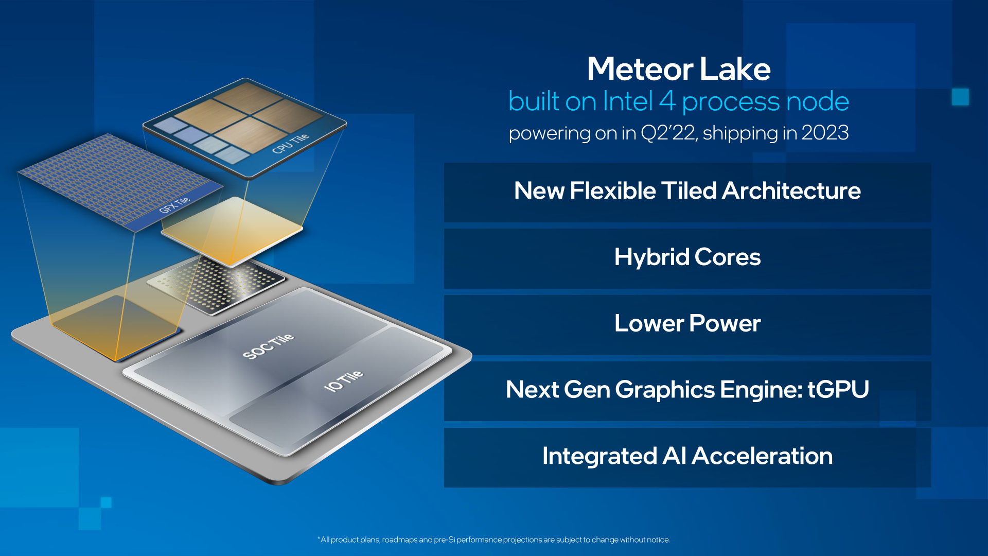
Intel 4, in flip, might be first used for Intel’s impending Meteor Lake shopper SoC, which is predicted to be the foundation of Intel’s 14th era Core processor circle of relatives. Although no longer transport till 2023, Intel already has Meteor Lake up and working of their labs, as according to the corporate’s conventional bring-up task. Together with brining an important bump in task applied sciences, Meteor Lake may also be Intel’s first tiled/chiplet-based shopper CPU, the use of a mixture of tiles for I/O, CPU cores, and GPU cores.
Intel 4 Bodily Parameters: 2x Density Over Intel 7, Cobalt Use Continues
Diving into the Intel 4 task, Intel has got down to take on a couple of various things right here. At the beginning is, after all, density. Intel is striving to stay Moore’s Legislation alive, and whilst the coinciding dying of Dennard scaling signifies that it’s now not a easy subject of lighting fixtures up two times as many transistors on each era, a better transistor density provides smaller chips at with the similar {hardware}, or throwing in additional cores (or different processing {hardware}) with more recent desgins.
| Evaluating Intel 4 to Intel 7 | |||
| Intel 4 | Intel 7 | Trade | |
| Fin Pitch | 30 nm | 34 nm | 0.88 x |
| Touch Gate Poly Pitch | 50 nm | 54/60 nm | 0.83 x |
| Minimal Steel Pitch (M0) | 30 nm | 40 nm | 0.75 x |
| HP Library Top | 240h | 408h | 0.59 x |
| Space (Library Top x CPP) | 12K nm2 | 24.4K nm2 | 0.49 x |
Of the figures Intel is freeing on this week’s paper, the fin pitch on Intel 4 is right down to 30nm, 0.88x the scale of Intel 7’s 34nm pitch. In a similar way, the pitch between touch gates is now 50nm, down from 60nm sooner than. However most importantly, the minimal steel pitch for the bottom layer (M0) may be 30nm, 0.75x the scale of the M0 pitch on Intel 7.
Intel’s library peak has additionally been lower down as neatly. The cellular peak for the high-performance library on Intel 4 is 240nm, which is most effective 0.59 x the peak of an HP cellular on Intel 7.
In consequence, Intel is claiming a 2x building up in density for Intel 4 as opposed to Intel 7 – or extra in particular, a halving of dimension for transistors – a conventional, complete node’s growth in transistor density.
Since chips are 2D constructs, the metric Intel makes use of for that is multiplying the HP cellular peak via the contacted poly pitch, which is largely the width of a cellular. If so they get 24,408 nm2 for Intel 7, and a flat 12,000 nm2 for Intel 4, 0.49x the realm of the Intel 7-based cellular.
In fact, no longer each form of construction scales via the similar issue with a brand new task node, and Intel 4 is not any other. In step with the corporate SRAM cells on Intel 4 are most effective round 0.77x the scale of the similar cells on Intel 7. So whilst standardized good judgment cells have doubled in density, SRAM density (for an identical SRAM sorts) has most effective progressed via 30% or so.
And, sadly, whilst Intel is speaking about density with admire to straightforward cells, they aren’t formally disclosing exact transistor density figures. For now, what Intel is telling us is that the full transistor density interprets neatly with the 2x determine they’re recently offering. Which, in keeping with what we learn about Intel 7 and its 80 million transistors according to mm2 density for HP libraries, would position Intel 4’s HP libraries at round 160MTr/mm2.
Since those figures are for Intel’s decrease density high-performance libraries, the most obvious follow-up query to that might be what the figures are for top density libraries – which historically squeeze issues much more in trade for lowered clockspeeds. Alternatively because it seems, Intel gained’t be creating excessive density libraries for Intel 4. As an alternative, Intel 4 might be a natural high-performance node, and high-density designs will include the successive node, Intel 3.
This peculiar construction comes on account of Intel’s modularization efforts for task node construction. Intel has necessarily followed a tick tock-like technique for node construction over the following part decade or so, with Intel creating an preliminary node in keeping with a brand new generation (e.g. EUV or Prime-NA machines), after which following that up with a extra subtle/optimized successor. Relating to Intel 4, whilst it’s doing necessary pioneering paintings for EUV inside of Intel’s fabs, the corporate’s larger plans are for Intel 3 to be their long-term, long-lived EUV node.
All of because of this that Intel has little need for high-density libraries with Intel 4, since it’s slated to get replaced with the extra fully-featured Intel 3 inside of a yr or so. And because Intel 3 is design appropriate with Intel 4, it’s transparent to look how Intel is pushing its personal design groups to make use of the latter task on every occasion timetables permit. Intel Foundry Services and products shoppers may also be a in a equivalent boat – they can use Intel 4, however IFS is extra keen on supplying get admission to to and design assist with Intel 3.
Getting again to Intel 4 itself, the brand new node comes with an important alternate to the steel layers as in comparison to Intel’s 10nm processes. Intel famously changed copper with cobalt on the lowest layers of its 10nm task, one thing that the corporate deemed vital for transistor longevity (electromigration resistance) causes. Sadly, cobalt isn’t as excellent from a functionality (clockspeed) viewpoint, and it’s lengthy been suspected that the transfer to cobalt was once some of the primary obstacles in 10nm construction for Intel.
For Intel 4, in flip, Intel is taking part a step again. The corporate remains to be the use of cobalt of their processes, however now somewhat than natural cobalt they’re the use of what they’re calling Enhanced Copper (eCu), which is copper cladded with cobalt. The speculation at the back of eCu is to have the most efficient of each phrases, keeping up the functionality of a doped copper metallization layer, whilst nonetheless getting the electromigration resistance advantages of cobalt.
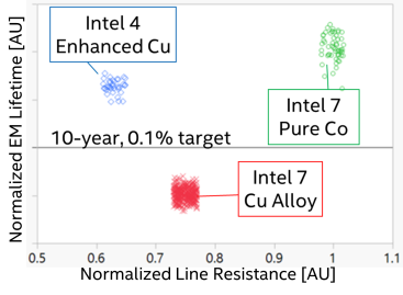
Electromigration lifetimes and line Resistance are when put next for various metallurgy choices.
And whilst Intel is now not the use of natural cobalt, in some respects their use of cobalt is expanding general. While Intel’s 10nm processes most effective used cobalt for the touch gate and primary two steel layers, Intel 4 is increasing the usage of eCu to the primary 5 steel layers. In consequence, the lowest-third of the whole steel layer stack in a chip is the use of Intel’s cobalt-clad copper. Intel has, on the other hand, got rid of cobalt from the gate itself; that’s now natural tungsten, somewhat than a mixture of tungsten and cobalt.
| Intel 4 Steel Stack | ||
| Layer | Steel | Pitch |
| Fin | – | 30 nm |
| Gate | Tungsten | 50 nm |
| Steel 0 | Copper w/Cobalt Cladding | 30 nm |
| Steel 1 | Copper w/Cobalt Cladding | 50 nm |
| Steel 2 | Copper w/Cobalt Cladding | 45 nm |
| Steel 3 | Copper w/Cobalt Cladding | 50 nm |
| Steel 4 | Copper w/Cobalt Cladding | 45 nm |
| Steel 5, 6 | Copper | 60 nm |
| Steel 7, 8 | Copper | 84 nm |
| Steel 9, 10 | Copper | 98 nm |
| Steel 11, 12 | Copper | 130 nm |
| Steel 13, 14 | Copper | 160 nm |
| Steel 15 | Copper | 280 nm |
| Large Steel 0 | Copper | 1080 nm |
| Large Steel 1 | Copper | 4000 nm |
All instructed, the selection of steel layers for Intel 4 has higher as opposed to Intel 7. While the latter had 15 steel layers for good judgment, Intel 4 squeezes in a 16th layer. That is joined via the standard two layers for persistent routing, which Intel phrases its large layers because of their reasonably huge pitches of 1080nm and 4000nm.
Along the tighter gate and steel layer pitches, some other house the place Intel is gaining density enhancements from design rule adjustments for interconnects. With Intel 4, Intel has moved to what they’re calling a gridded interconnect design, which briefly, most effective lets in for vias going between steel layers to be positioned according to a pre-determined grid. Up to now, vias might be positioned any place, which allowed for some flexibility, however had different trade-offs.
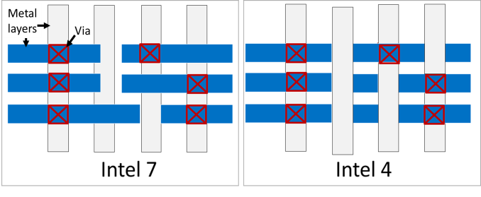
Design regulations modified from conventional (left) to gridded (proper) to give a boost to yield and give a boost to functionality although capacitance aid
In step with Intel, the usage of grids has progressed each the yields of the method via decreasing variability, in addition to how they cross about optimizing designs. The transfer additionally has an aspect advantage of permitting Intel to steer clear of having to make use of advanced, multi-patterned EUV for his or her interconnects.
After all, as in the past discussed, the usage of EUV may be permitting Intel to cut back the selection of steps (and the selection of mask) required to fab a chip. Whilst the corporate isn’t providing absolute numbers, on a relative foundation Intel 4 calls for 20% fewer mask than Intel 7. Had Intel no longer accomplished this, the selection of mask required would have as an alternative shot up via round 30% because of the selection of multi-patterning steps required.
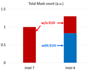
In depth employment of EUV permits function scaling and task simplification
The usage of EUV may be having a good affect on Intel’s yields. Although the corporate isn’t offering precise numbers, the aid within the selection of steps provides fewer alternatives for the rest to head incorrect that might introduce a defect on a wafer.
Intel 4 Efficiency: 21.5% Extra Perf at iso-power/40% Much less Energy at iso-frequency
Density enhancements apart, what sort of functionality enhancements is Intel seeing for the Intel 4 task? In brief, Intel is seeing above-average beneficial properties in each frequencies and gear potency.
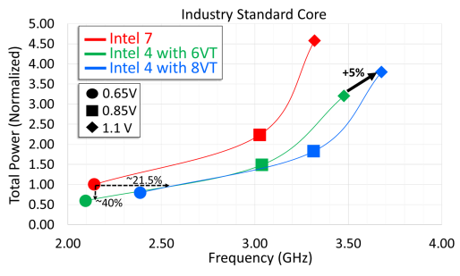
Circuit research of business usual core displays 21.5% functionality acquire at matched persistent over Intel 7 at 0.65V. 8VT glide permits 5% functionality acquire over 6VT at excessive voltages.
At an iso-power of 0.65v, Intel is seeing a 21.5% building up in clockspeeds possible as opposed to Intel 7. With that mentioned, 0.65v is on the low finish of the curve, and Intel’s graph does display diminishing returns as you cross farther up in voltage; at 0.85v and past the iso-power beneficial properties are nearer to ten%. In step with Intel, they are able to squeeze out some other 5% or so via the use of cells designed for upper threshold voltages (8VT), which comes at a price of upper general persistent intake as opposed to usual cells.
And if we take issues from the opposite finish, Intel is reporting even greater beneficial properties at the persistent potency entrance with Intel 4. At iso-frequency – on this case round 2.1GHz – Intel is seeing 40% decrease persistent intake. There are once more diminishing returns as frequencies building up (up till Intel 7 hits its sensible limits), but it surely’s extra constant than the functionality/frequency beneficial properties. This mirrors what we’ve noticed with different task nodes – together with Intel 7 at its release – the place more recent nodes are decreasing persistent intake at a far higher fee than they’re enabling upper clockspeeds. A complete CPU constructed at the Intel 4 task may conceivably save an excessive amount of persistent – as long as you don’t thoughts it no longer clocking any upper than sooner than.
All instructed, the functionality beneficial properties defined in Intel’s paper reflect the ones that they’ve been claiming up till now, such because the 20% perf-per-watt beneficial properties for Intel 4 mentioned ultimately summer season’s task roadmap replace. For the remaining yr Intel has been drawing near the completing line for Intel 4 construction, in order their paper outlines, they look like on-track for turning in on their functionality beneficial properties.
In the meantime, Intel may be reporting excellent traits in price scaling from Intel 7 to Intel 4, although as soon as once more the corporate isn’t offering particular numbers. 1 EUV layer does finally end up being dearer than 1 DUV layer, however as a result of EUV gets rid of a number of multi-patterning, it is helping to carry down the entire prices via decreasing the entire selection of steps. The transfer to EUV may be decreasing a little bit of the capital force on Intel, as Intel 4 doesn’t require relatively as a lot blank room house (although it’s certainly not a small quantity general).
In the long run, as Intel seems to send Meteor Lake and different first-generation Intel 4 merchandise in 2023, what is still noticed is how briefly Intel can get their new task node up and working to the criteria of high-volume production. With Meteor Lake samples already in Intel’s labs, Intel is getting ever nearer to in spite of everything getting into the EUV age. However for Intel, hitting all in their objectives getting there way no longer simply scaling up manufacturing from their Hillsboro construction fab, but in addition mastering the fascinating activity of replicating their task to Eire and the opposite Intel fabs that might be used for Intel 4.
Supply Through https://www.anandtech.com/display/17448/intel-4-process-node-in-detail-2x-density-scaling-20-improved-performance