
Because the darkish of the night time rolls into China this night time, Qualcomm is internet hosting a mobile-focused product release tournament they’re calling “Snapdragon Evening”. Headlining the development is the announcement of the corporate’s new flagship SoC, the Snapdragon 8+ Gen 1. A mid-generation replace to their flagship smartphone SoC, the Snapdragon 8 Gen 1, the 8+ Gen 1 follows Qualcomm’s annual custom of liberating a refresh product to spice up efficiency and to provide companions one thing new to paintings with for the second one part of the 12 months. And for this 12 months particularly, we’re having a look at an excessively notable trade in chips from Qualcomm.
In contrast to earlier generations the place Qualcomm simply introduced a quicker velocity bin in their current silicon, for 2022 we have now one thing extra considerable to speak about. Qualcomm has switched up foundries completely – shifting from Samsung to TSMC – and because of this is rolling out a brand new die. Due to this, the Snapdragon 8+ Gen 1 Qualcomm is reaping one thing of a one-off production acquire, permitting them to each dial up CPU and GPU efficiency whilst concurrently chopping chronic intake.
| Qualcomm Snapdragon 8 Gen 1 Flagship SoCs | |||
| SoC | Snapdragon 8+ Gen 1 | Snapdragon 8 Gen 1 | |
| CPU | 1x Cortex-X2 @ 3.2GHz 3x Cortex-A710 4x Cortex-A510 6MB sL3 |
1x Cortex-X2 @ 3.0GHz 3x Cortex-A710 4x Cortex-A510 6MB sL3 |
|
| GPU | Adreno (10% Upper Clockspeed) |
Adreno | |
| DSP / NPU | Hexagon | Hexagon | |
| Reminiscence Controller |
4x 16-bit CH
@ 3200MHz LPDDR5 / 51.2GB/s 4MB machine point cache |
||
| ISP/Digital camera | Triple 18-bit Spectra ISP
1x 200MP or 108MP with ZSL 8K HDR video & 64MP burst seize |
||
| Encode/ Decode |
8K30 / 4K120 10-bit H.265
Dolby Imaginative and prescient, HDR10+, HDR10, HLG 720p960 endless recording |
||
| Built-in Modem | X65 built-in
(5G NR Sub-6 + mmWave) |
||
| Mfc. Procedure | TSMC 4nm | Samsung 4nm | |
Temporarily diving into the specs, the brand new Snapdragon 8+ Gen 1 is basically the unique Snapdragon 8 Gen 1 ported over from Samsung’s 4nm line over to one in every of TSMC’s 4nm traces. Below extra customary instances, this type of a shift would most probably be unremarkable – or at maximum, an a laugh workout in on the lookout for edge circumstances – alternatively for Qualcomm’s flagship SoC, the subject is extra vital.
Whilst reliable assets and statements at the high quality of Samsung’s 4nm procedure are few and some distance between, unofficially, it’s turn into transparent that Samsung’s 4nm procedure hasn’t lived as much as expectancies. This has brought about a cascading affect at the chips made at the procedure node, resulting in the unique Snapdragon 8 Gen 1 creating an affinity for chronic intake, and Samsung’s personal Exynos 2200 no longer faring any higher. Conversely, by way of all accounts TSMC’s N4 procedure is having a look nice, with the optically gotten smaller node construction off of TSMC’s already a hit and really performant 5nm applied sciences.
Because of this efficiency hole between Samsung and TSMC’s 4nm nodes, Qualcomm is taking the strange step of (necessarily) porting their high-end SoC over to TSMC’s fab. Which, even supposing no longer strictly essential – Qualcomm carries numerous momentum and the 8 Gen 1 has been promoting smartly – is unquestionably a prudent transfer for the corporate. Qualcomm is going through particularly stiff festival this era from MediaTek, whose flagship-level Dimensity 9000 SoC used to be the lead product for TSMC’s 4nm node. And that leaves MediaTek with a definite benefit in opposition to the unique 8 Gen 1, one who Qualcomm can be more than pleased to nullify.
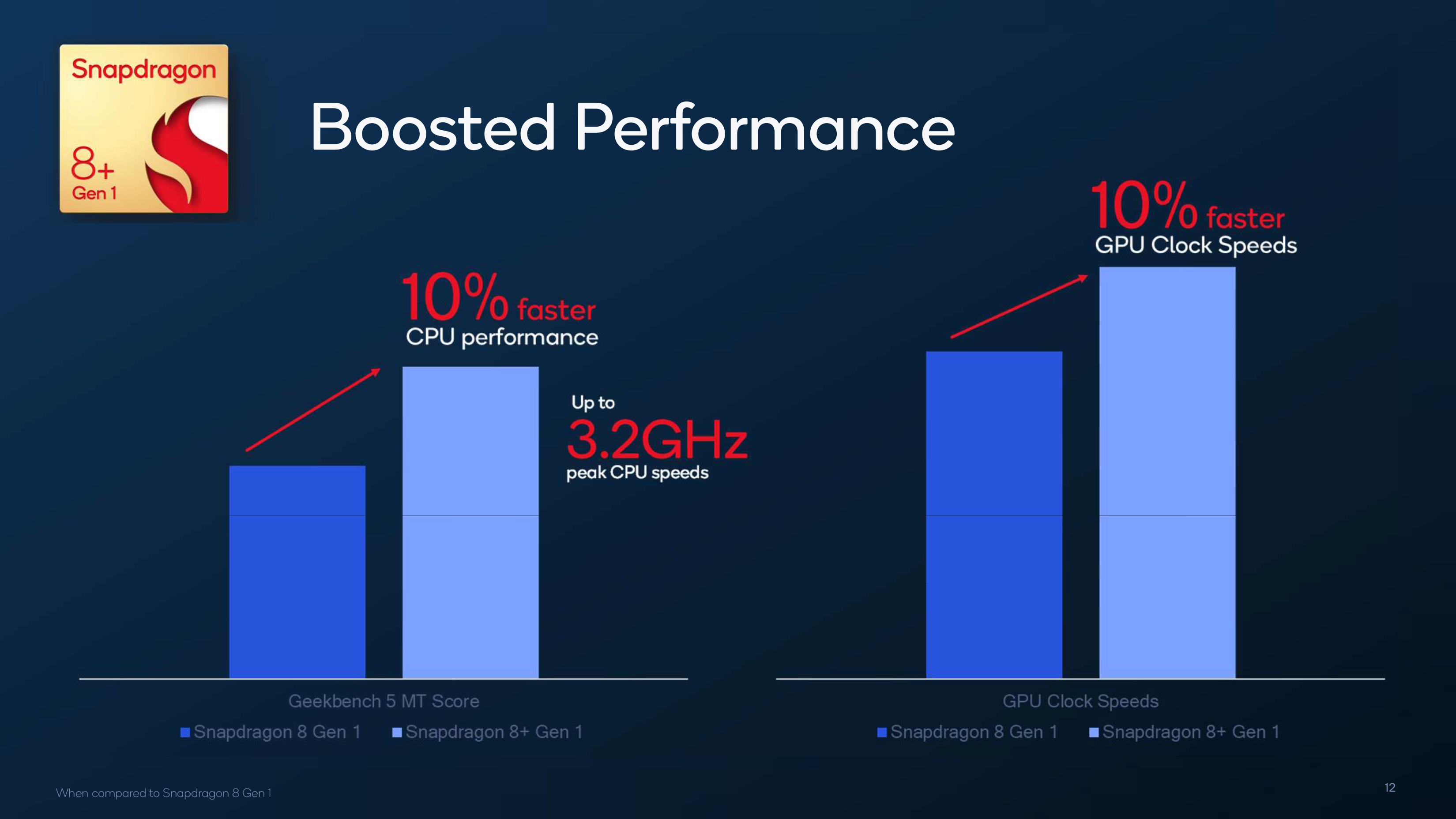
In the end, the transfer in fabs is giving Qualcomm an opportunity to strengthen upon the unique 8 Gen 1 from each ends of the spectrum, ensuing within the Snapdragon 8+ Gen 1. At the efficiency entrance, TSMC’s node presents them a very easy alternative to extend CPU and GPU clockspeeds for extra efficiency. The high Cortex-X2 core is now clocked 7% upper, at 3.2GHz, and in the meantime the A710 and A510 clusters have observed their clockspeeds dialed up much more considerably, by way of round 12% each and every. Now even the slowest A510 cores can run at 2GHz. GPU clockspeeds have additionally been in a similar way larger, and whilst Qualcomm does no longer expose explicit clockspeeds there, they’ve showed that the 8+ Gen 1’s Adreno GPU block is clocked 10% upper than the unique 8 Gen 1.
However, if anything else, the majority of Qualcomm’s positive factors from the transfer in production nodes are being invested in chopping chronic intake. One thing of a sore level with the 8 Gen 1, TSMC’s higher 4nm procedure implies that Qualcomm is seeing a lot decrease chronic intake throughout their SoC at iso-frequency.
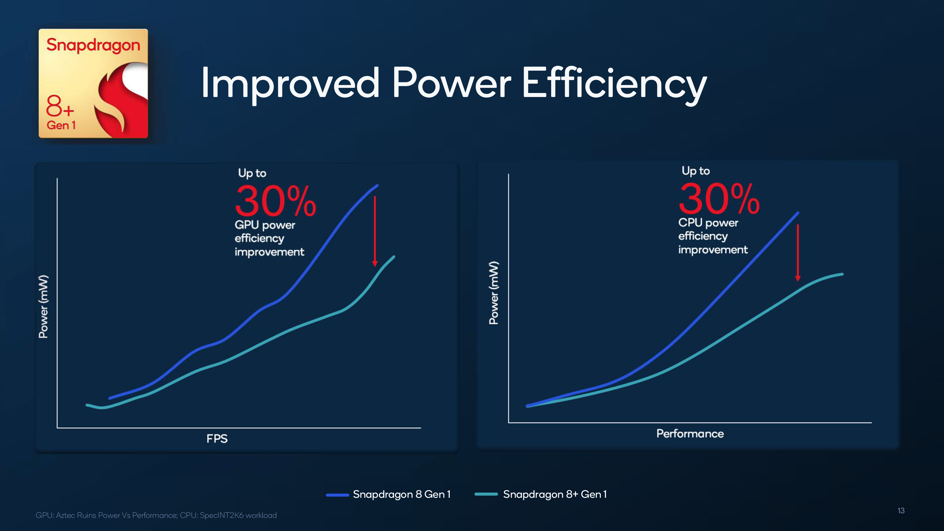
Formally, Qualcomm is claiming a 30% development in each GPU and CPU chronic potency. Even though as discussed prior to, that is at iso-frequency and doesn’t remember the upper height clockspeeds of the 8+ Gen 1. Because of this, the real-world chronic financial savings aren’t going to be relatively as nice on a peak-to-peak foundation, however consistent with Qualcomm the facility financial savings are nonetheless vital. General, the corporate is touting a fifteen% relief in SoC chronic utilization beneath “sensible utilization patterns” as opposed to the unique 8 Gen 1, which in flip must result in stepped forward battery lifetimes in handsets that undertake the brand new SoC.
Previous that, the reliable specs for the 8+ Gen 1 don’t mirror any subject material adjustments to the SoC’s configuration as opposed to the unique chip. So we’re nonetheless having a look on the identical built-in X65 5G modem, the similar Spectra ISP, and the similar video encode/decode blocks (sorry, gang, nonetheless no AV1 fortify!). So, in spite of assembling a brand new die for his or her mid-generation refresh product this 12 months, there aren’t any new options to talk of with the 8+ Gen 1.
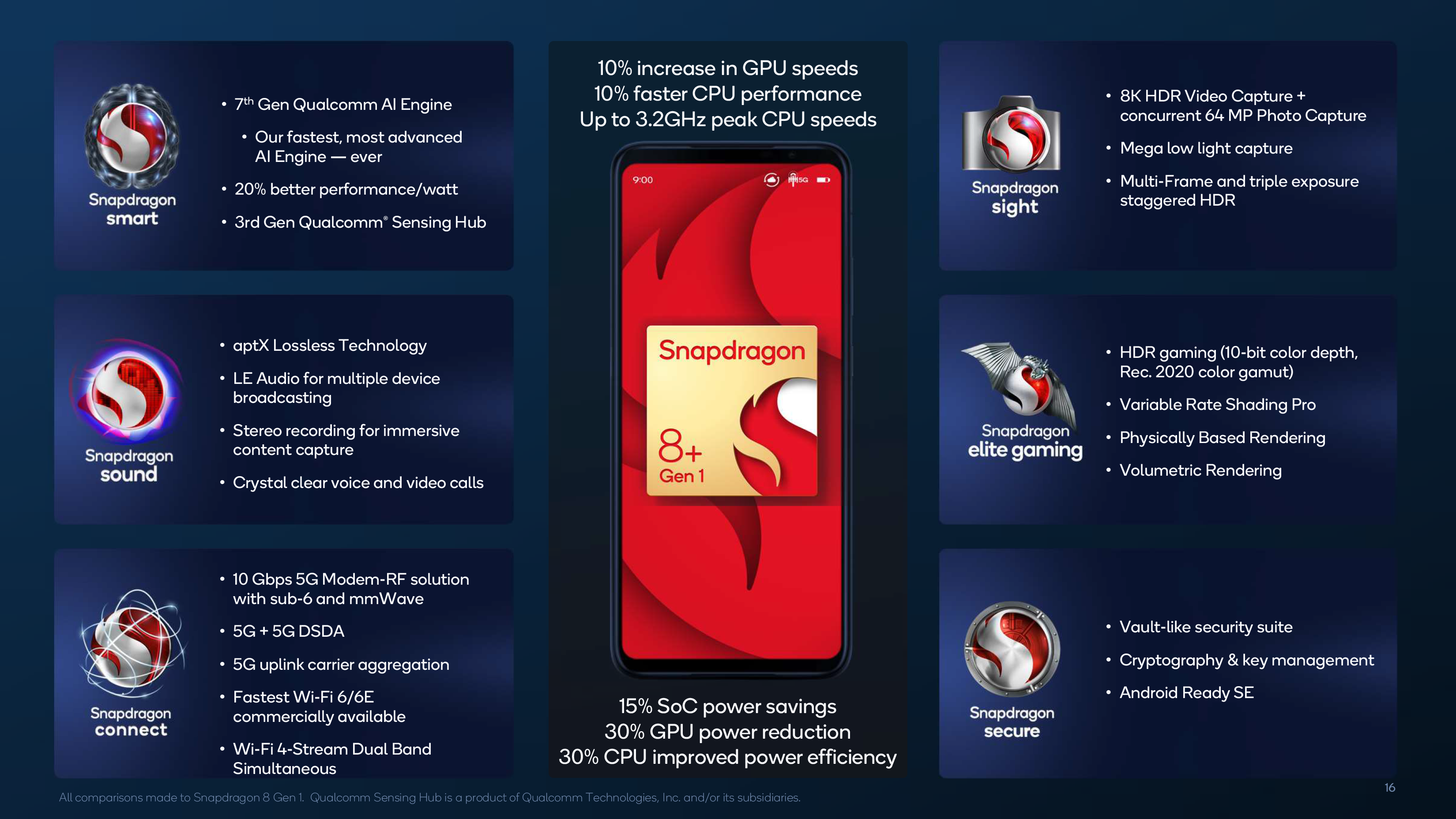
As for SoC efficiency, formally Qualcomm is claiming 10% stepped forward GPU and CPU efficiency, owing to these aforementioned clockspeed will increase. Whilst we weren’t in a position to wait a benchmarking consultation that Qualcomm held closing week, the Efficiency Mode figures being launched by way of the corporate are kind of in-line with those claims. Qualcomm’s Geekbench 5 effects are a number of % upper than what we benchmarked again in December on the 8 Gen 1 release tournament, although it’s notable that they didn’t succeed in meaningfully upper rankings in PCMark. GPU efficiency figures are in a similar way blended, with a few of Qualcomm’s reliable effects coming very just about our authentic 8 Gen 1 effects, however I’m reluctant to learn an excessive amount of into them given how a lot if a distinction height as opposed to sustained trying out makes in GPU effects. As all the time, the ultimate will want to come right down to impartial, third-party trying out, although at face price not anything Qualcomm claims is unreasonable given the clockspeed enhancements and the thermal headroom received from the transfer to TSMC.
After all, as for customers, they’ll be capable of get their first have a look at Snapdragon 8+ Gen 1 gadgets in Q3 of this 12 months. Consistent with Qualcomm, most of the same old suspects have signed directly to free up telephones in response to the brand new SoC, together with Asus, Motorola, OnePlus, Honor, and Xiaomi.
Supply By means of https://www.anandtech.com/display/17395/qualcomm-announces-snapdragon-8-gen-1-moving-to-tsmc-for-more-speed-lower-power