Whilst this yr’s Spring GTC tournament doesn’t function any new GPUs or GPU architectures from NVIDIA, the corporate remains to be within the means of rolling out new merchandise in keeping with the Hopper and Ada Lovelace GPUs its offered up to now yr. On the high-end of the marketplace, the corporate these days is pronouncing a brand new H100 accelerator variant particularly geared toward vast language fashion customers: the H100 NVL.
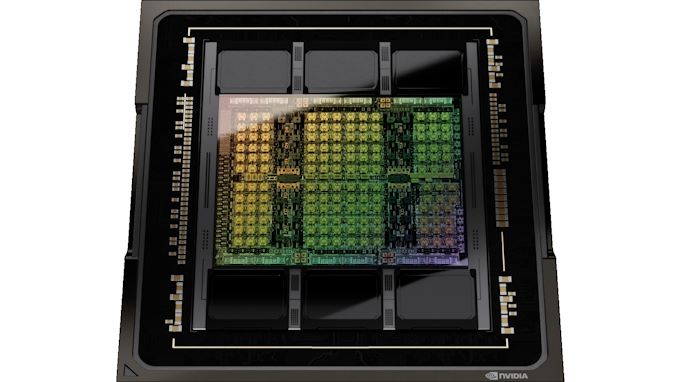
The H100 NVL is a fascinating variant on NVIDIA’s H100 PCIe card that, in an indication of the days and NVIDIA’s intensive luck within the AI box, is geared toward a unique marketplace: vast language fashion (LLM) deployment. There are some things that make this card odd from NVIDIA’s standard server fare – now not the least of which is that it’s 2 H100 PCIe forums that come already bridged in combination – however the giant takeaway is the large reminiscence capability. The mixed dual-GPU card gives 188GB of HBM3 reminiscence – 94GB consistent with card – providing extra reminiscence consistent with GPU than another NVIDIA section up to now, even inside the H100 circle of relatives.
| NVIDIA H100 Accelerator Specification Comparability | |||||
| H100 NVL | H100 PCIe | H100 SXM | |||
| FP32 CUDA Cores | 2 x 16896? | 14592 | 16896 | ||
| Tensor Cores | 2 x 528? | 456 | 528 | ||
| Spice up Clock | 1.98GHz? | 1.75GHz | 1.98GHz | ||
| Reminiscence Clock | ~5.1Gbps HBM3 | 3.2Gbps HBM2e | 5.23Gbps HBM3 | ||
| Reminiscence Bus Width | 6144-bit | 5120-bit | 5120-bit | ||
| Reminiscence Bandwidth | 2 x 3.9TB/sec | 2TB/sec | 3.35TB/sec | ||
| VRAM | 2 x 94GB (188GB) | 80GB | 80GB | ||
| FP32 Vector | 2 x 67 TFLOPS? | 51 TFLOPS | 67 TFLOPS | ||
| FP64 Vector | 2 x 34 TFLOPS? | 26 TFLOPS | 34 TFLOPS | ||
| INT8 Tensor | 2 x 1980 TOPS | 1513 TOPS | 1980 TOPS | ||
| FP16 Tensor | 2 x 990 TFLOPS | 756 TFLOPS | 990 TFLOPS | ||
| TF32 Tensor | 2 x 495 TFLOPS | 378 TFLOPS | 495 TFLOPS | ||
| FP64 Tensor | 2 x 67 TFLOPS? | 51 TFLOPS | 67 TFLOPS | ||
| Interconnect | NVLink 4 (600GB/sec) |
NVLink 4 (600GB/sec) |
NVLink 4 18 Hyperlinks (900GB/sec) |
||
| GPU | 2 x GH100 (814mm2) |
GH100 (814mm2) |
GH100 (814mm2) |
||
| Transistor Depend | 2 x 80B | 80B | 80B | ||
| TDP | 700-800W | 350W | 700W | ||
| Production Procedure | TSMC 4N | TSMC 4N | TSMC 4N | ||
| Interface | 2 x PCIe 5.0 (Quad Slot) |
PCIe 5.0 (Twin Slot) |
SXM5 | ||
| Structure | Hopper | Hopper | Hopper | ||
Riding this SKU is a selected area of interest: reminiscence capability. Huge language items just like the GPT circle of relatives are in lots of respects reminiscence capability certain, as they’ll temporarily refill even an H100 accelerator with the intention to dangle all in their parameters (175B in terms of the biggest GPT-3 items). Consequently, NVIDIA has opted to scrape in combination a brand new H100 SKU that gives somewhat extra reminiscence consistent with GPU than their standard H100 portions, which most sensible out at 80GB consistent with GPU.
Underneath the hood, what we’re taking a look at is basically a unique bin of the GH100 GPU that’s being put on a PCIe card. All GH100 GPUs include 6 stacks of HBM reminiscence – both HBM2e or HBM3 – with a capability of 16GB consistent with stack. On the other hand for yield causes, NVIDIA most effective ships their common H100 portions with 5 of the 6 HBM stacks enabled. So whilst there’s nominally 96GB of VRAM on every GPU, most effective 80GB is to be had on common SKUs.

The H100 NVL, in flip, is the legendary fully-enabled SKU with all 6 stacks enabled. Through turning at the 6th HBM stack, NVIDIA is in a position to get right of entry to the extra reminiscence and extra reminiscence bandwidth that it gives. It’ll have some subject material affect on yields – how a lot is a carefully guarded NVIDIA secret – however the LLM marketplace is it appears sufficiently big and prepared to pay a excessive sufficient top rate for almost highest GH100 applications to make it value NVIDIA’s whilst.
Even then, it will have to be famous that consumers aren’t gaining access to slightly all 96GB consistent with card. Quite, at a complete capability of 188GB of reminiscence, they’re getting successfully 94GB consistent with card. NVIDIA hasn’t long gone into element in this design quirk in our pre-briefing forward of these days’s keynote, however we suspect this could also be for yield causes, giving NVIDIA some slack to disable unhealthy cells (or layers) inside the HBM3 reminiscence stacks. The online result’s that the brand new SKU gives 14GB extra reminiscence consistent with GH100 GPU, a 17.5% reminiscence building up. In the meantime the mixture reminiscence bandwidth for the cardboard stands at 7.8TB/2nd, which matches out to three.9TB/2nd for the person forums.
But even so the reminiscence capability building up, in numerous tactics the person playing cards inside the greater dual-GPU/dual-card H100 NVL glance so much just like the SXM5 model of the H100 put on a PCIe card. While the traditional H100 PCIe is hamstrung some by way of slower HBM2e reminiscence, fewer energetic SMs/tensor cores, and decrease clockspeeds, the tensor core efficiency figures NVIDIA is quoting for the H100 NVL are all at parity with the H100 SXM5, indicating that this card isn’t additional reduce like the traditional PCIe card. We’re nonetheless ready at the ultimate, whole specs for the product, however assuming the whole lot here’s as introduced, then the GH100s going into the H100 NVL would constitute the very best binned GH100s these days to be had.
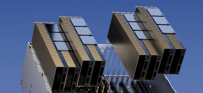
And an emphasis at the plural is named for right here. As famous previous, the H100 NVL isn’t a unmarried GPU section, however moderately it’s a dual-GPU/dual-card section, and it items itself to the host device as such. The {hardware} itself is in keeping with two PCIe form-factor H100s which are strapped in combination the use of 3 NVLink 4 bridges. Bodily, that is nearly similar to NVIDIA’s present H100 PCIe design – which will already be paired up the use of NVLink bridges – so the variation isn’t within the development of the 2 board/4 slot behemoth, however moderately the standard of the silicon inside of. Put differently, you’ll be able to strap in combination common H100 PCie playing cards these days, nevertheless it wouldn’t fit the reminiscence bandwidth, reminiscence capability, or tensor throughput of the H100 NVL.
Unusually, regardless of the stellar specifications, TDPs stay virtually. The H100 NVL is a 700W to 800W section, which breaks right down to 350W to 400W consistent with board, the decrease certain of which is similar TDP because the common H100 PCIe. On this case NVIDIA seems to be to be prioritizing compatibility over height efficiency, as few server chassis can care for PCIe playing cards over 350W (and less nonetheless over 400W), which means that TDPs wish to stand pat. Nonetheless, given the upper efficiency figures and reminiscence bandwidth, it’s unclear how NVIDIA is affording the additional efficiency. Energy binning can cross far right here, nevertheless it can be a case the place NVIDIA is giving the cardboard the next than standard spice up clockspeed for the reason that target audience is essentially considering tensor efficiency and isn’t going to be lighting fixtures up all the GPU directly.
Differently, NVIDIA’s choice to unencumber what’s necessarily the most efficient H100 bin is an peculiar selection given their basic choice for SXM portions, nevertheless it’s a call that is sensible in context of what LLM consumers want. Huge SXM-based H100 clusters can simply scale as much as 8 GPUs, however the quantity of NVLink bandwidth to be had between any two is hamstrung by way of the wish to undergo NVSwitches. For only a two GPU configuration, pairing a collection of PCIe playing cards is a lot more direct, with the mounted hyperlink making certain 600GB/2nd of bandwidth between the playing cards.
However in all probability extra importantly than this is merely an issue of with the ability to temporarily deploy H100 NVL in present infrastructure. Quite than requiring putting in H100 HGX provider forums particularly constructed to pair up GPUs, LLM consumers can simply toss H100 NVLs in new server builds, or as a fairly fast improve to present server builds. NVIDIA goes for an excessively explicit marketplace right here, in the end, so the traditional good thing about SXM (and NVIDIA’s talent to throw its collective weight round) would possibly not practice right here.
All advised, NVIDIA is touting the H100 NVL as providing 12x the GPT3-175B inference throughput as a last-generation HGX A100 (8 H100 NVLs vs. 8 A100s). Which for purchasers taking a look to deploy and scale up their techniques for LLM workloads as temporarily as imaginable, is indubitably going to be tempting. As famous previous, H100 NVL doesn’t convey anything else new to the desk with regards to architectural options – a lot of the efficiency spice up right here comes from the Hopper structure’s new transformer engines – however the H100 NVL will serve a selected area of interest because the quickest PCIe H100 possibility, and the choice with the biggest GPU reminiscence pool.
Wrapping issues up, in step with NVIDIA, H100 NVL playing cards will start delivery in the second one part of this yr. The corporate isn’t quoting a value, however for what’s necessarily a most sensible GH100 bin, we’d be expecting them to fetch a most sensible value. Particularly in gentle of the way the explosion of LLM utilization is popping into a brand new gold rush for the server GPU marketplace.
Supply Through https://www.anandtech.com/display/18780/nvidia-announces-h100-nvl-max-memory-server-card-for-large-language-models