
At GTC 2023, Nvidia introduced its new cuLitho tool library for dashing up a essential bottleneck within the semiconductor production workflow. The brand new library speeds computational lithography, one way used to create photomasks for chip manufacturing. Nvidia claims its new manner allows 500 DGX H100 methods wielding 4,000 Hopper GPUs to do the same quantity of labor as 40,000 CPU-based servers, however accomplish that 40X quicker and with 9X much less energy. Nvidia claims this reduces the computational lithography workload to provide a photomask from a number of weeks down to 8 hours.
Chipmaking leaders TSMC, ASML, and Synopsys have all signed on for the brand new tech, with Synopys already integrating it into its tool design equipment. Over the years, Nvidia expects the brand new technique to allow upper chip density and yield, higher design laws, and AI-powered lithography.
Nvidia scientists created new algorithms that let increasingly-complex computational lithography workflows to execute on GPUs in parallel, showing a 40X speedup the use of Hopper GPUs. The brand new algorithms are built-in into a brand new cuLitho acceleration library that may be built-in into masks makers’ tool (most often a foundry or a chip dressmaker). The cuLitho acceleration library could also be appropriate with Ampere and Volta GPUs, despite the fact that Hopper is the quickest resolution.

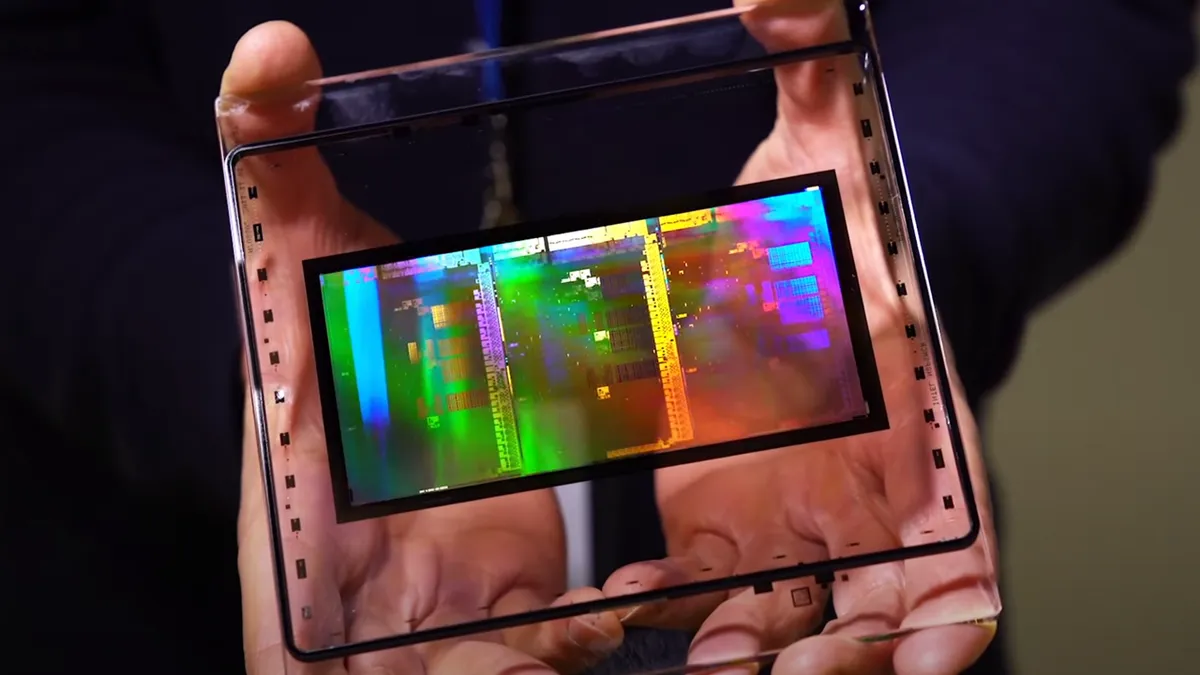
Printing the small options on a chip begins with a bit of quartz referred to as a photomask. This clear quartz has an imprinted development of a chip design and works just like a stencil — shining a gentle throughout the masks etches the design onto the wafer, thus developing the billions of 3-d transistors and twine constructions that contain a contemporary chip. Each and every chip design calls for more than one exposures to increase the chip’s design in layers. As such, the collection of photomasks used all over the chipmaking job varies in accordance with the chip; it will possibly even exceed 100 mask. As an example, Nvidia says it takes 89 mask to create the H100, and Intel cites ’50+’ mask used for its 14nm chips.
New ways have emerged that now permit etching options smaller than the wavelength of the sunshine used to create them. Then again, the continuing shrinkage of the options has resulted in problems with diffraction, which necessarily ‘blurs’ the design that is being revealed onto the silicon. The sphere of computational lithography counteracts the have an effect on of diffraction thru advanced mathematical operations that optimize the masks structure. Then again, this activity is changing into more and more compute-intensive as options shrink even additional, thus enabling billions extra transistors consistent with design.
Those advanced issues require huge clusters of computer systems, steadily numbering tens of hundreds of servers (Nvidia cites 40,000), that crunch throughout the numbers in parallel on CPUs in a workload that may take as much as weeks to job a unmarried photomask (the period of time varies in accordance with chip complexity — Intel says it takes its workforce 5 days to create a unmarried masks).
Nvidia contends that the collection of servers required to design a contemporary masks is expanding on the identical price as Moore’s Legislation, thus pushing the server necessities and the volume of energy had to perform them into unsustainable territory. Actually, the unbelievable compute necessities for brand new masks tech, like Inverse Lithography Generation (ILT) which makes use of Inverse Curvilinear Mask (ILM), has already hampered the adoption of those extra complex ways. Moreover, Prime-NA EUV and ILT are anticipated to extend the volume of information processing for mask by means of 10X within the coming years.
Symbol 1 of 2
That is the place Nvidia’s cuLitho steps in, decreasing the computational lithography workload to 8 hours. The cuLitho library may also be built-in into computational lithography tool that leverages ILT (curvilinear shapes) or Optical Proximity Correction (OCP, which makes use of ‘New york’ shapes) ways, and is already built-in into Synopsys’ equipment. TSMC and ASML also are adopting the tech. Given the sensitivity of those types of tool, US export controls will govern any distribution of the tool to China and different areas matter to sanctions.
Intel has lengthy used its personal proprietary tool equipment however is slowly transferring to adopting industry-standard equipment, specifically because it starts enforcing its personal exterior IDM 2.0 foundry operations. As such, it’s but to be noticed if different large fabs, like Intel and Samsung, will undertake the brand new tool for their very own interior equipment. Regardless, the reinforce from Synopsys, ASML, and TSMC assures vast uptake of the cuLitho library and Nvidia’s GPU-based answers with main semiconductor producers over the approaching years.
Supply Through https://www.tomshardware.com/information/nvidia-tackles-chipmaking-process-claims-40x-speed-up-with-culitho