Taiwan Semiconductor Production Co. on Thursday kicked off its 2022 TSMC Era Symposium, the place the corporate historically stocks it job era roadmaps in addition to its long term growth plans. One of the vital key issues that TSMC is pronouncing nowadays are its modern nodes that belong to its N3 (3 nm category) and N2 (2nm category) households that will probably be used to make complex CPUs, GPUs, and SoCs within the coming years.
Contents
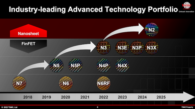
N3: 5 Nodes Over Subsequent 3 Years
As fabrication processes get extra advanced, their pathfinding, analysis, and building occasions get stretched out as smartly, so we now not see a brand-new node rising each and every two years from TSMC and different foundries. With N3, TSMC’s new node advent cadence goes to enlarge to round 2.5 years, while with N2, it is going to stretch to round 3 years.
Because of this TSMC will wish to be offering enhanced variations of N3 with a purpose to meet the desires of its shoppers who’re nonetheless searching for a functionality in step with watt growth in addition to transistor density bump annually or so. One more reason why TSMC and its shoppers want a couple of variations of N3 is since the foundry’s N2 will depend on all-new gate-all-around field-effect transistors (GAA FETs) carried out the use of nanosheets, which is predicted to return with upper prices, new design methodologies, new IP, and plenty of different adjustments. Whilst builders of bleeding-edge chips will probably be fast to leap to N2, lots of TSMC’s extra rank & document shoppers will keep on with more than a few N3 applied sciences for years yet to come.
At its TSMC Era Symposium 2022, the foundry mentioned 4 N3-derived fabrication processes (for a complete of 5 3 nm-class nodes) — N3E, N3P, N3S, and N3X — set to be presented over the approaching years. Those N3 variants are slated to ship advanced job home windows, upper functionality, higher transistor densities, and augmented voltages for ultra-high-performance programs. A lot of these applied sciences will toughen FinFlex, a TSMC “secret sauce” function that very much complements their design flexibility and permits chip designers to exactly optimize functionality, energy intake, and prices.
| Marketed PPA Enhancements of New Procedure Applied sciences Information introduced throughout convention calls, occasions, press briefings and press releases |
||||||||
| TSMC | ||||||||
| N4 vs N5 |
N4P vs N5 |
N4P vs N4 |
N4X vs N5 |
N4X vs N4P |
N3 vs N5 |
N3E vs N5 |
||
| Energy | decrease | -22% | – | ? | ? | -25-30% | -34% | |
| Efficiency | upper | +11% | +6% | +15% or extra |
+4% or extra |
+10-15% | +18% | |
| Good judgment Space
Aid* % Good judgment Density* |
0.94x
-6% 1.06x |
0.94x
-6% 1.06x |
– |
? |
? |
0.58x
-42% 1.7x |
0.625x
-37.5% 1.6x |
|
| Quantity Production |
2022 | 2023 | H2 2022 | 2023 | 2023 | H2 2022 | Q2/Q3 2023 | |
*Notice that TSMC simplest began to post transistor density improvements for analog, common sense, and SRAM one by one round 2020. One of the crucial numbers nonetheless replicate ‘combined’ density consisting of fifty% common sense, 30% SRAM, and 20% analog.
N3 and N3E: On Monitor for HVM
TSMC’s first 3 nm-class node is known as N3 and this one is on course to begin excessive quantity production (HVM) in the second one part of this 12 months. Precise chips are set to be dropped at shoppers in early 2023.This era is most commonly geared toward early adopters (learn: Apple and the like) who can spend money on modern designs and would have the benefit of the functionality, energy, space (PPA) benefits introduced via modern nodes. However as it is adapted for specific sorts of programs, N3 has a fairly slim job window (a variety of parameters that produce an outlined consequence), which will not be appropriate for all programs with regards to yields.
That is when N3E comes into play. The brand new era complements functionality, lowers energy, and will increase the method window, which leads to upper yields. However the trade-off is that the node includes a quite decreased common sense density. When in comparison to N5, N3E will be offering a 34% relief in energy intake (on the identical pace and complexity) or an 18% functionality growth (on the identical energy and complexity), and can building up common sense transistor density via 1.6x.
It’s noteworthy that, in accordance with knowledge from TSMC, N3E will be offering upper clockspeeds than even N4X (due in 2023). On the other hand the latter will even toughen ultra-high force currents and voltages of above 1.2V, at which level it is going to have the ability to be offering unbeatable functionality, however with very excessive energy intake.
Basically, N3E appears to be a extra flexible node than N3, which is why it isn’t unexpected that TSMC has extra ‘3nm tape outs’ at this level than it had with its 5 nm-class node at a identical level of its building.
Chance manufacturing of chips the use of N3E is about to begin within the coming weeks (i.e., in Q2 or Q3 2022) with HVM set for mid-2023 (once more, TSMC does no longer reveal whether or not we’re speaking about Q2 or Q3). So be expecting industrial N3E chips to be to be had in past due 2023 or early 2024.
N3P, N3S, and N3X: Efficiency, Density, Voltages
N3’s enhancements don’t forestall with N3E. TSMC is about to convey out N3P, a performance-enhanced model of its fabrication job, in addition to N3S, density-enhancing taste of this node, a while round 2024. Sadly, TSMC isn’t recently disclosing what enhancements those variants will be offering in comparison to baseline N3. In reality, at its Era Symposium 2022, TSMC didn’t even display N3S in its roadmap and it simplest were given discussed via Kevin Zhang in a dialog. Bearing all this in thoughts, it’s in point of fact no longer a excellent trade to take a look at guessing traits of N3S.
In the end, for the ones shoppers who want ultra-high functionality regardless of energy intake and prices, TSMC will be offering N3X, which is basically an ideological successor of N4X. Once more, TSMC isn’t revealing information about this node instead of that it is going to toughen excessive force currents and voltages. We may speculate that N4X may use bottom energy supply, however since we’re speaking a few FinFET-based node and TSMC simplest going to put in force bottom energy rail in nanosheet-based N2, we don’t seem to be positive that is the case. However, TSMC almost certainly has various aces up its sleeve in the case of voltage will increase and function improvements.
FinFlex: N3’s Secret Sauce
Talking of improvements, we will have to surely point out TSMC’s secret sauce for N3: FinFlex era. In brief, FinFlex permits chip designers to exactly tailor their development blocks for upper functionality, upper density, and decrease energy.
Replace 6/17: The preliminary model of the tale incorrectly referred same old cells and blocks as transistors, which has been corrected.
When the use of a FinFET-based node, chip designers can make a choice from other libraries the use of other same old cells. A typical mobile is essentially the most elementary development block that plays a Boolean common sense or garage serve as and is composed of a bunch of transistors and interconnects. From math viewpoint, the similar serve as can also be carried out (with the similar consequence) the use of an ordinary mobile of various configurations. However from manufacturability and operation viewpoint, other same old mobile configurations are characterised via other functionality, energy intake, and space. When builders wish to reduce die dimension and save energy at the price of functionality, they use small same old cells. But if they wish to maximize functionality on the trade-off of die dimension and better energy, they use massive same old cells.
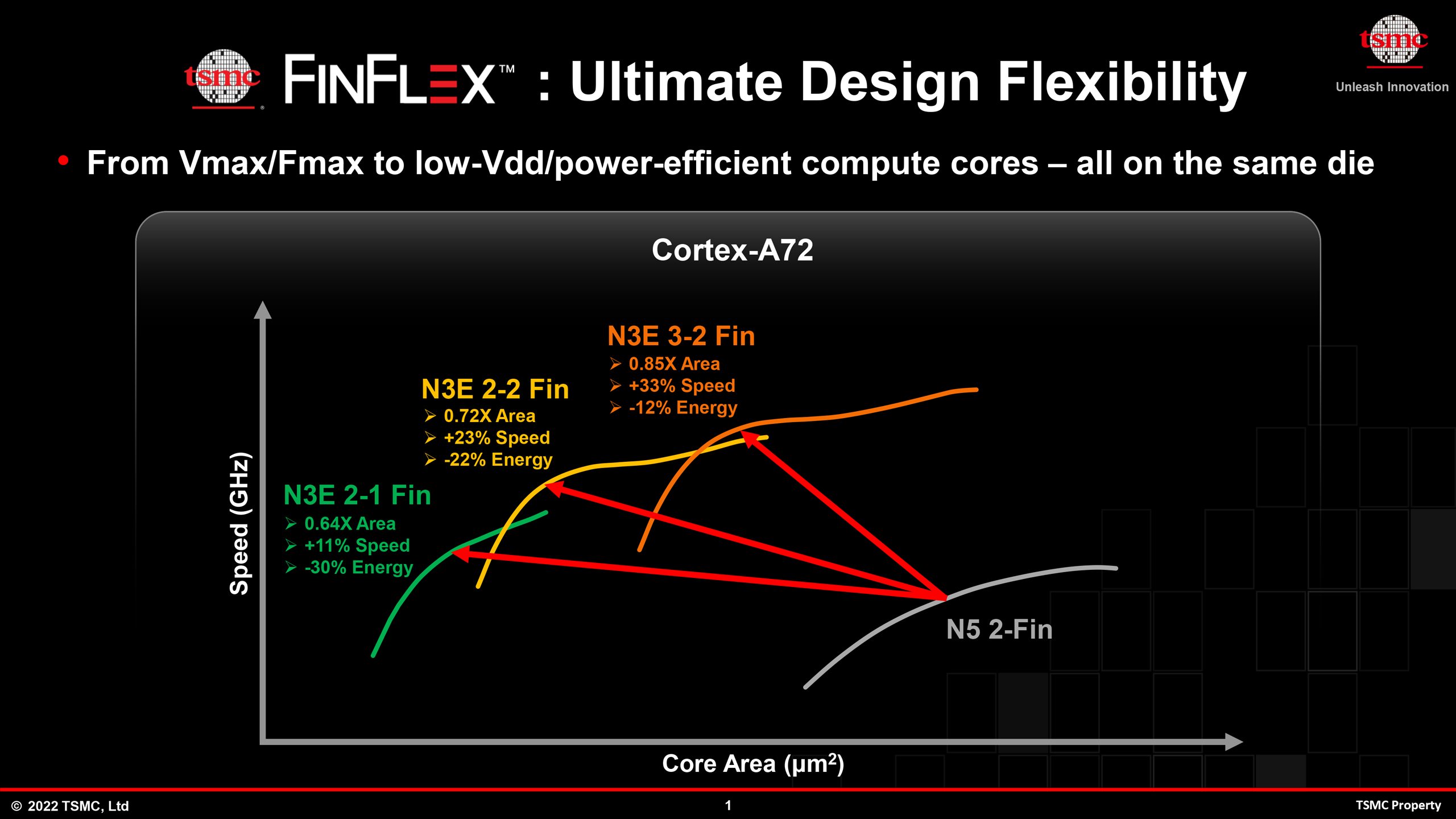
These days, chip designers must keep on with one library/same old cells both for the entire chip or the entire block in a SoC design. As an example, CPU cores can also be carried out the use of 3-2 fin blocks to lead them to run quicker, or 2-1 fin same old cells to scale back their energy intake and footprint. It is a honest tradeoff, however it is not perfect for all circumstances, particularly after we are speaking about 3 nm-class nodes that will probably be dearer to make use of than present applied sciences.
For N3, TSMC’s FinFlex era will permit chip designers to mix ‘n match other sorts of same old cells inside one block to exactly tailor functionality, energy intake, and space. For advanced constructions like CPU cores, such optimizations give numerous alternatives to extend core functionality whilst nonetheless optimizing die sizes. So, we’re keen to look how SoC designers will have the ability to make the most of FinFlex within the looming N3 generation.
FinFlex isn’t an alternative to node specialization (functionality, density, voltages) as job applied sciences have higher variations than the ibraries or transistor constructions inside a unmarried job era, however FinFlex appears to be an effective way to optimize functionality, energy, and prices for TSMC’s N3 node. In the end, this era will convey the versatility of FinFET-based nodes somewhat nearer to that of nanosheet/GAAFET-based nodes, which might be slated to supply adjustable channel widths to get upper functionality or scale back energy intake.
Abstract
Like TSMC’s N7 and N5, N3 will probably be some other circle of relatives of long-lasting nodes for the sector’s biggest distinction maker of semiconductors. Particularly with the bounce to nanosheet-based GAAFETs arising at 2nm for TSMC, the 3nm circle of relatives would be the ultimate circle of relatives of “vintage” modern FinFET nodes from the company, and one who numerous shoppers will keep on with for a number of years (or extra). Which, in flip, is why TSMC is prepping a couple of variations of N3 adapted for various programs – in addition to FinFlex era to present chip designers some further flexibility with their designs.
The primary N3 chips are set to go into manufacturing within the coming months and arrive to the marketplace in early 2023. In the meantime, TSMC will stay generating semiconductors the use of its N3 nodes lengthy after it introduces its N2 job era in 2025.
Supply Via https://www.anandtech.com/display/17452/tsmc-readies-five-3nm-process-technologies-with-finflex