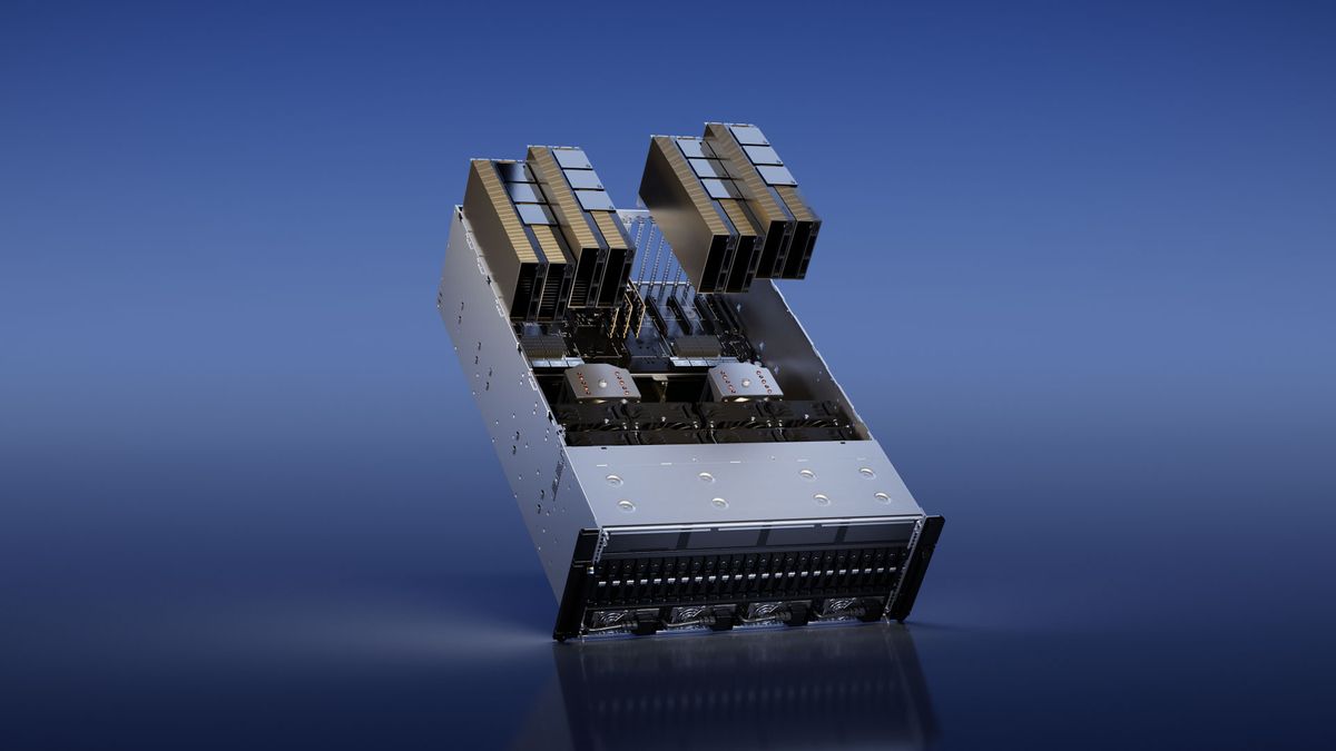
Nvidia introduced a brand new dual-GPU product, the H100 NVL, all over its GTC Spring 2023 keynote. This would possibly not deliver again SLI or multi-GPU gaming, and would possibly not be probably the most easiest graphics playing cards for gaming, however as an alternative objectives the rising AI marketplace. From the tips and pictures Nvidia has launched, the H100 NVL (H100 NVLink) will recreation 3 NVLink connectors at the best, with the 2 adjoining playing cards slotting into separate PCIe slots.
Notice that the present H100 PCIe already had the 3 NVLink choices, however the H100 NVL makes another adjustments and also will most effective be bought as a paired card answer. It is a fascinating exchange of tempo, it sounds as if to deal with servers that do not reinforce Nvidia’s SXM possibility, with a focal point on inference efficiency reasonably than coaching. The NVLink connections will have to assist give you the lacking bandwidth that NVSwitch offers at the SXM answers, and there are another notable variations as neatly.
Take the specs. Earlier H100 answers — each SXM and PCIe — have include 80GB of reminiscence (HBM3 for the SXM, HBM2e for PCIe), however the real bundle comprises six stacks, each and every with 16GB of reminiscence. It isn’t transparent if one stack is totally disabled, or if it is for ECC or another objective. What we do know is that the H100 NVL will include 94GB in step with GPU, and 188GB HBM3 overall. We think the “lacking” 2GB in step with GPU is both for ECC or come what may associated with yields, even though the latter turns out slightly strange.
Energy is moderately upper than the H100 PCIe, at 350–400 watts in step with GPU (configurable), an building up of 50W. General efficiency in the meantime finally ends up being successfully double that of the H100 SXM: 134 teraflops of FP64, 1,979 teraflops of TF32, and seven,916 teraflops FP8 (in addition to 7,916 teraops INT8).
Principally, this looks as if the similar core design of the H100 PCIe, which additionally helps NVLink, however doubtlessly now with extra of the GPU cores enabled, and with 17.5% extra reminiscence. The reminiscence bandwidth could also be fairly slightly upper than the H100 PCIe, because of the transfer to HBM3. H100 NVL tests in at 3.9 TB/s in step with GPU and a blended 7.8 TB/s (as opposed to 2 TB/s for the H100 PCIe, and three.35 TB/s at the H100 SXM).
As it is a dual-card answer, with each and every card occupying a 2-slot area, Nvidia most effective helps 2 to 4 pairs of H100 NVL playing cards for spouse and licensed methods. How a lot would a unmarried pair price, and can they be to be had to buy one by one? That is still observed, even though a unmarried H100 PCIe can once in a while be discovered for round $28,000 (opens in new tab). So $80,000 for a couple of H100 NVL does not appear out of the query.
Supply By way of https://www.tomshardware.com/information/nvidia-dual-gpu-h100-nvl